
Bypassing Tangem Card Security with a Laser Attack
After uncovering a genuine check bypass on the Tangem Android application and a brute-force attack on the card's authentication protocol, the Ledger Donjon turned its attention to the card itself with more advanced tools and sophisticated techniques. What we found is a critical vulnerability that lets an attacker with physical access to a single Tangem card reset its password and steal all associated funds.
TL;DR
— Using a single nanosecond laser pulse targeted at a specific location on the EAL6+ chip, the Ledger Donjon demonstrated a fault injection attack against Tangem hardware wallet cards. By evading the platform’s fault-detection countermeasures and faulting a single conditional check in Tangem’s firmware, we set the card’s access password to an attacker-controlled value.
— The vulnerability does not require knowledge of the existing password or possession of a backup card, and is not mitigated by disabling the recovery feature.
— The vulnerability affects all Tangem cards currently in circulation and cannot be patched, as the cards have no firmware update mechanism.1
— To be clear, the attack requires physical access to the Tangem card, and pulling off the attack demands specialized laboratory equipment (our setup costs around $250,000), software and hardware security expertise, and an extensive initial effort to characterize the chip, none of which is within reach of an individual attacker.
The vulnerability was disclosed to Tangem on February 10th, 2026.
Tangem Wallet - A credit card that holds your crypto
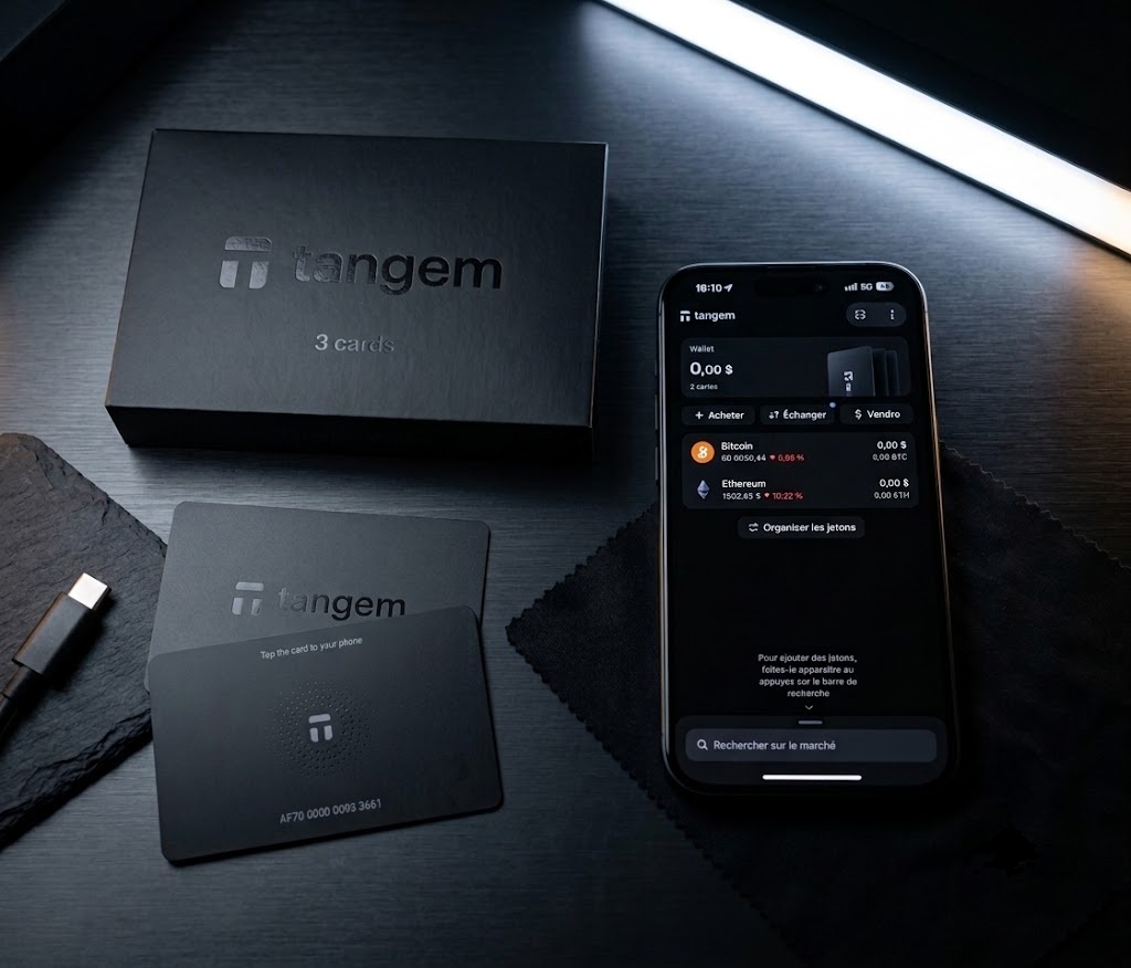
Tangem wallets look and feel like ordinary credit cards. Inside, a Samsung S3D232A secure element which is certified to EAL6+2 handles key generation, storage, and transaction signing. The chip communicates with a companion mobile app over NFC. The master key never leaves the card. Therefore, physical access to the card and knowledge of the configured password are the two factors that gate access to the funds linked to the master key.
The security-critical logic lives in Tangem’s own closed-source firmware, which runs directly on the secure element and cannot be inspected or reverse-engineered. The Samsung S3D232A platform is just as opaque, as no documentation, peripheral datasheets, tooling, or firmware are publicly available. The system therefore operates as a near-complete black box, protected by an EAL6+ certified chip designed to resist hardware tampering. The Tangem mobile app is open source3, which does expose the list of supported APDU instructions and gives us a useful map of the command interface.
How Tangem Wallet password recovery works
Tangem wallets are sold in sets of two or three cards that share the same master key after onboarding them together. If you lose your password, a recovery mechanism, enabled by default on every card, lets you reset it as long as you physically hold two cards linked together during the onboarding process. The mobile application orchestrates a challenge-response protocol between those two cards. Then the recovered card enters a special state that allows a password change using the SetPin instruction without providing the old one. (Although the instruction name and its TLV tags refer to a “PIN”, the data exchanged is actually the password digest rather than a numeric PIN.)
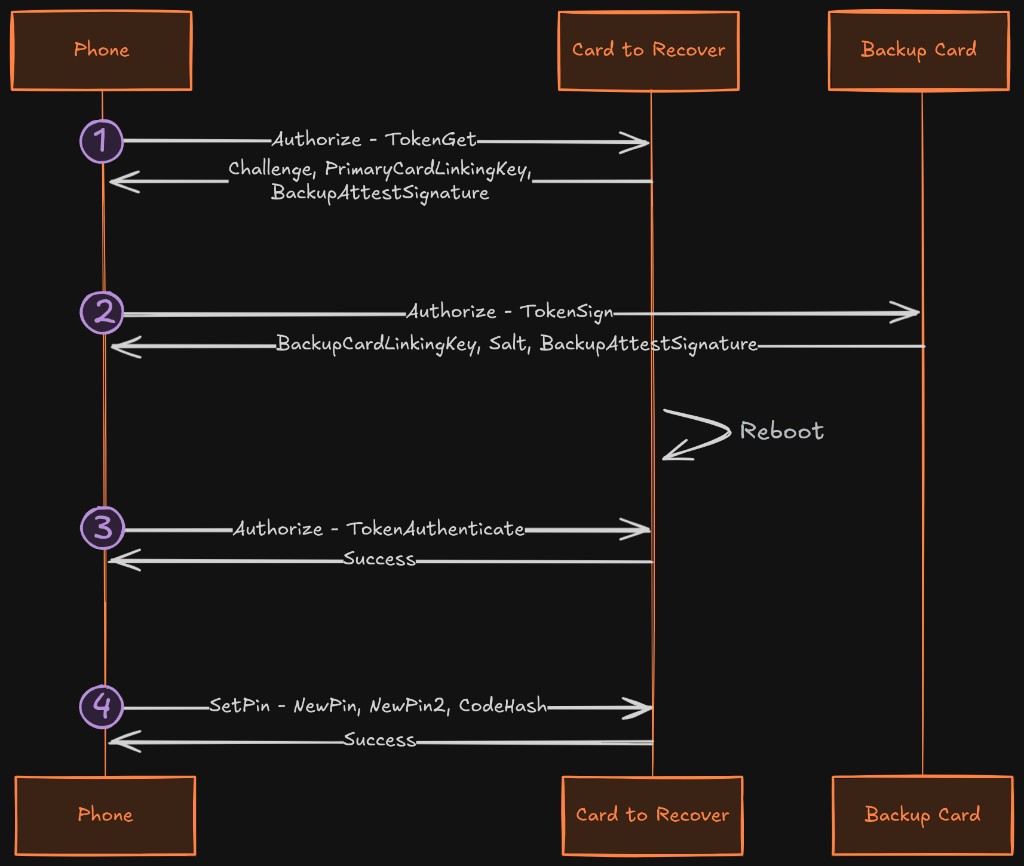
This feature introduces a distinct code path inside the SetPin instruction handler (step 4). Somewhere in this instruction’s logic, there must be a conditional check: “is this card in recovery state?” If so, the new password is accepted without the previous one. If not, the command is rejected unless the correct previous password is provided.
If this assumption holds, then a potential attack path emerges: we can try to fault this single condition so the card accepts a new password without actually being in recovery state. Since the goal of the fault is to bypass the recovery state check itself, the three preceding steps of the recovery flow, which only serve to legitimately set that state, become irrelevant. The attack only requires sending a SetPin instruction with a new password, without the previous one and without a backup card. Furthermore, unlike authentication commands that typically impose delays or lockouts after repeated failures, SetPin applies no such penalty, enabling an unrestricted number of rapid attempts.
Setting up the attack
Step 1 - Creating a wired connection to a Tangem card
Before we can do anything interesting, we need better signals than what we had during our previous password brute-force attack. Tangem cards communicate exclusively over NFC (ISO 14443 Type A), which means the chip is powered inductively by a 13.56 MHz RF field. While this is perfectly fine for normal usage, it poses a significant challenge for hardware security evaluation: the AC power delivery introduces substantial noise on the power consumption measurements. The same applies to electromagnetic measurements, which are dominated by the RF carrier. Additionally, the power delivery is unstable, so the card constantly adapts its execution time (which is overall slower because less energy is delivered than in a full-contact setup). As a consequence, side-channel analysis and precise fault injection timing become very difficult.
We developed a two-stage technique: first, we solder the card chip onto a custom Scaffold daughterboard4 and wire its antenna directly into the impedance matching circuit, replacing inductive coupling with a wired connection. Then, during command processing, we switch power from the AC carrier to an external DC power supply. This yields significantly cleaner power and electromagnetic traces, enabling more precise timing analysis of the chip’s internal operations. It also makes the card execute commands roughly five times faster, directly increasing the throughput of fault injection campaigns.
Step 2 - Preparing the card by exposing its silicon die
The card’s plastic body is cut open with a scalpel. The metal shielding underneath is removed, along with the adhesive layer5, to expose the silicon die. One antenna connection is cut and rewired through our daughterboard.
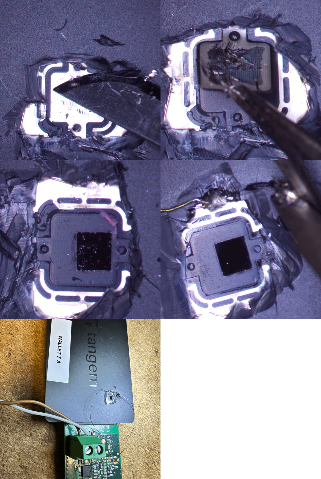
The card is now ready for further evaluation.
Step 3 - Conducting the attack
Given the target is a certified secure element with active countermeasures, we chose to start directly with laser fault injection rather than less invasive techniques such as voltage or electromagnetic glitching. Laser fault injection works by aiming a high-power-density pulse of infrared light at a specific location on the die, through the backside, at a precise moment during execution. The photon energy temporarily alters transistor states, which can disrupt the program’s intended flow, such as bypassing a conditional check. In our case, the target is the recovery state check inside the SetPin instruction handler.
Finding the password recovery conditional check timing
For side-channel analysis, we used a Langer EMV ICR electromagnetic probe positioned directly on the chip die and connected to an oscilloscope. The Tangem card is mounted on our custom NFC daughterboard and controlled by Scaffold, our in-house evaluation platform, which also provides integrated power consumption measurements. This setup allows us to capture both electromagnetic and power traces during command execution, providing the timing information needed to identify where the recovery state check occurs.
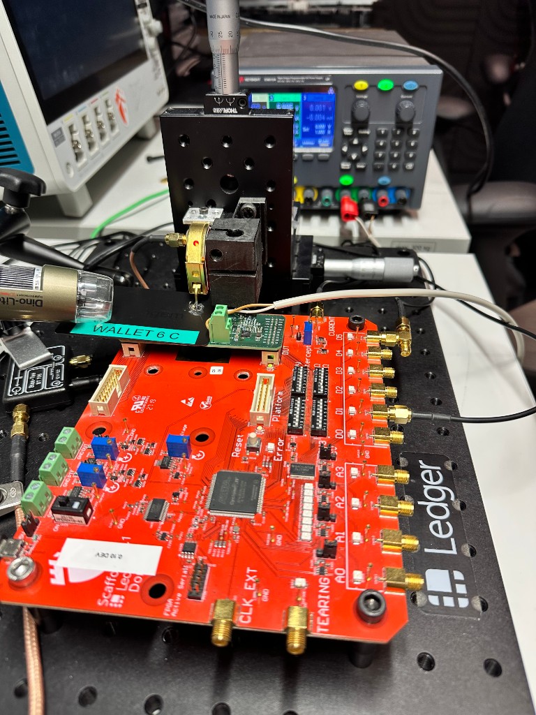
With better electromagnetic traces in hand thanks both to our sample preparation and setup, we need to answer one critical question: when does the card check the recovery state?
To do this, we acquired electromagnetic traces of the SetPin instruction execution under two scenarios:
- Legitimate recovery:
SetPinis run after the full recovery flow and the password reset is successful (all steps of the previous sequence diagram). - Unauthorized recovery attempt: only step 4 is performed;
SetPinis sent without prior authorization and without the old password, so the card returns an error since the recovery state is incorrect.
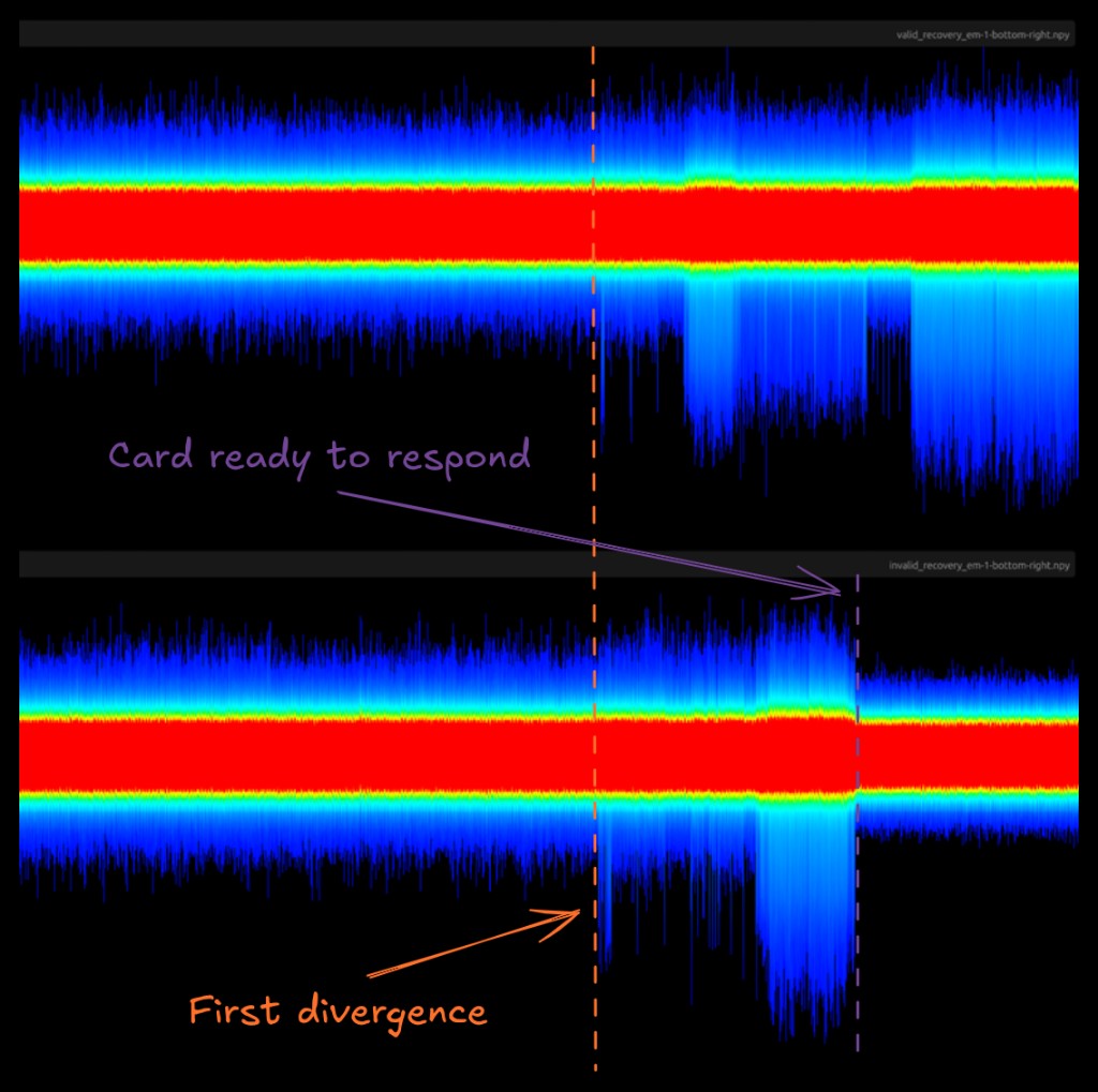
By comparing the electromagnetic traces from both scenarios, we identified a timing window where the execution paths diverge. The traces are identical up to the orange dotted line, as both executions process the same APDU payload in the same way, and only diverge from that point onward when the chip evaluates the recovery state. The window extends until the card begins transmitting the error status word in the invalid recovery case.
The actual branch decision likely occurs near the beginning of this window, but due to the timing jitter observed across acquisitions, we define a conservatively wider target window to ensure the fault has a chance to land on the check regardless of timing variation.
Flash write operations that brick the card
Successfully injecting a fault with a laser requires simultaneously satisfying three constraints: spatial (targeting the correct transistors on the die), temporal (firing during a narrow window of the instruction’s execution), and parametric (using appropriate laser power, pulse width, and spot size). Without knowledge of the chip’s internal layout or firmware implementation, this search space is prohibitively large to explore by brute force.
But that’s not all. We are operating in a black box, so what follows is our best interpretation of observed behavior rather than a confirmed mechanism. During early fault injection attempts, we observed recurring events on the power consumption traces that were absent during normal execution: brief, high-current draws consistent with flash write operations. These events appeared only when the laser was fired, which suggests the chip detects the perturbation and responds by writing to non-volatile memory.
Our working hypothesis is a persistent fault counter: each time a perturbation is detected (whether through hardware sensors, instruction-flow monitoring, or integrity checks), the chip increments a counter in flash. After roughly 256 such events, the cards we tested became permanently unresponsive and could not be recovered by power cycling. We cannot confirm the exact threshold or mechanism without access to the firmware.
Even if these flash writes were not a deliberate security counter, they would remain dangerous: any unexpected write to flash during command execution risks corrupting the card’s data or firmware. Either way, the consequence is the same: naive brute-forcing of the fault parameters is impossible. Therefore, we needed a way to retry without persisting any state, even when a perturbation is detected. For the remainder of this post we refer to these events as flash writes.
Evading flash writes via tearing
The key insight is that writing to flash takes time and produces a distinctive signature on the power consumption trace. If we can detect a flash write in real time and cut power at the very beginning of the operation, the write never completes and nothing gets persisted. Whether it was a fault counter increment or a write that would have corrupted the card, the result is the same: it’s as if it never happened. The card powers back up next time exactly in the state it was before. We still have to allow the flash write used to write the new password digest on successful fault injection.
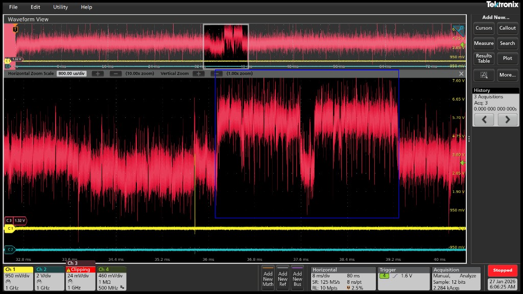
By using a FPGA-based card, we can monitor the secure element power consumption in real time and trigger an immediate power cut when it detects the flash write pattern in a specific timing window. This “power tearing” technique theoretically gives us unlimited retries.
In reality, the detection isn’t perfect. Flash writes might occur during the card’s response phase, and the response pattern looks very similar. We had to accept a trade-off with our current setup: allow responses through for fault characterization while accepting occasional counter increments. In practice, it extended card life from a few minutes to over a day which is more than enough to find our fault. Also, once the right parameters are found, getting the card’s response is not needed anymore making the probability of counter increment much lower.
Scanning the die
For laser fault injection, we use an AlphaNov laser bench equipped with a pulse driver module capable of generating nanosecond-scale pulses. The card remains wired on the NFC daughterboard connected to our Scaffold evaluation board. Scaffold is additionally connected to the custom FPGA-based re-synchronization card. An oscilloscope provides additional observability during injection campaigns.
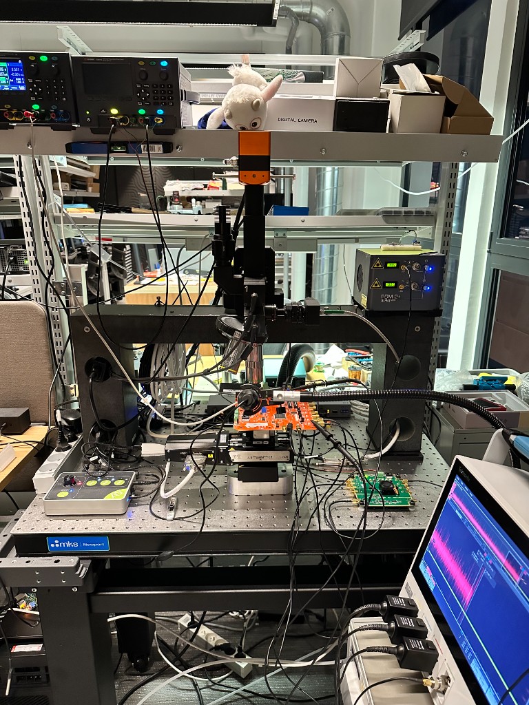
With the tearing setup in place, we swept the laser across the chip surface while randomizing timing, power, and pulse width. We initially focused on the flash memory and its address decoder, then on the RAM, but neither region produced useful results within our timing window. Faults in these areas either had no observable effect or systematically triggered fault detection, likely because these memories are protected by error-correcting codes (ECC). We then shifted focus to the glue logic area, which contains the chip’s combinational and sequential logic, and quickly identified some responsive regions.
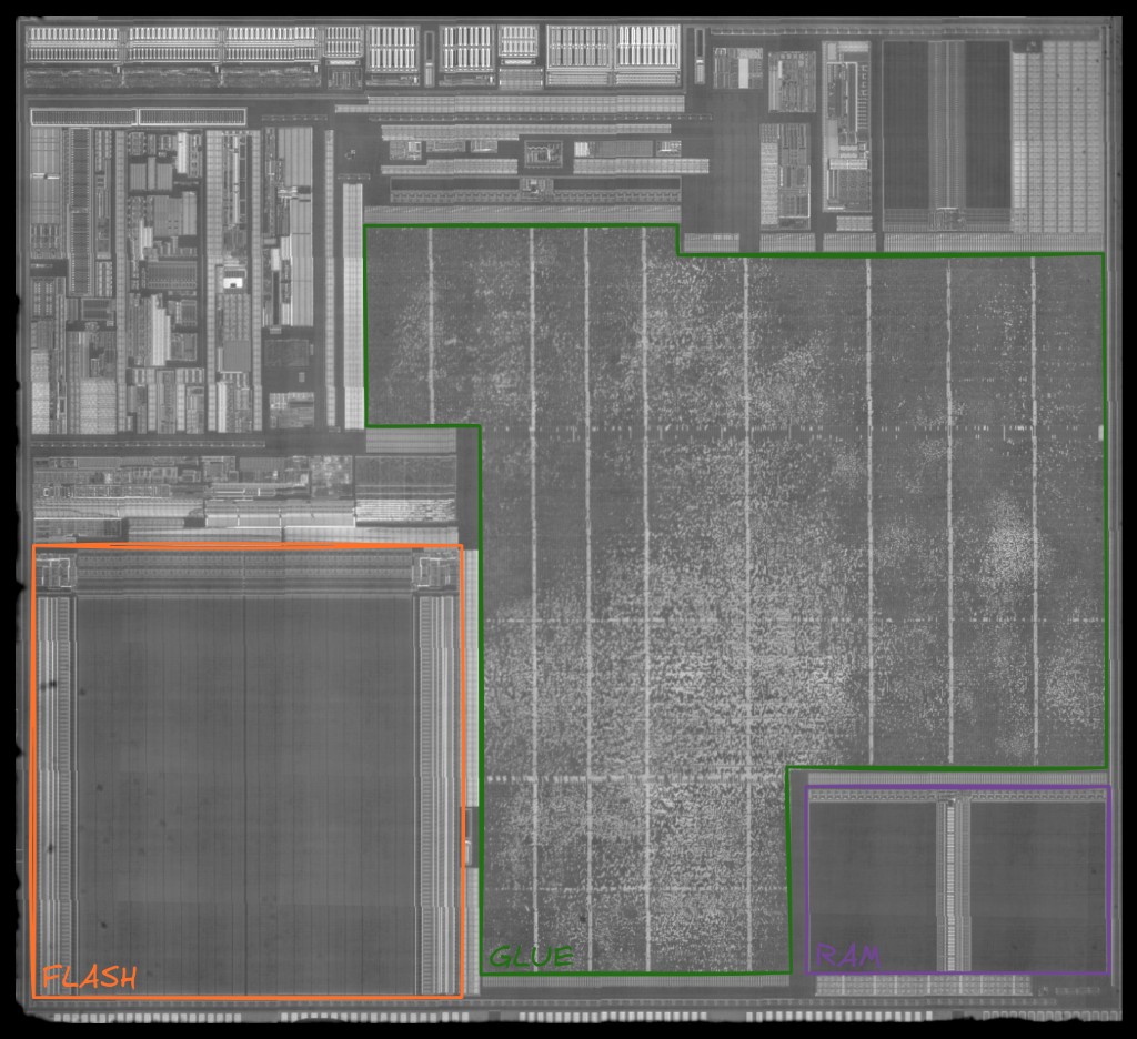
Potential ISO 7816 peripheral area
This area is very sensitive to laser pulses, but only corrupts the card’s response data without affecting execution logic. We observed what appeared to be uninitialized SRAM content leaking through corrupted buffer offsets, interesting, but not useful for our purposes.
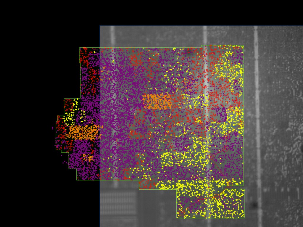
Potential instruction skip area
The exact location on the die is not disclosed in this publication.
This is where we found the most promising results. Faults in this region produced unusual status words such as 6A86 (“incorrect P1-P2 parameters” error) that are not normally returned during SetPin execution and that we believe originate from the Tangem firmware rather than the platform. Their timing is consistent with our expectation that the recovery-state check happens after class/instruction verification but before TLV data processing. Based on the nature of these perturbations and the status words returned, the observed effects are consistent with instruction skips or corrupted branch decisions within the software execution flow, though we cannot confirm this without access to the firmware source code.
Having identified the right region and timing neighborhood, we narrowed the scan accordingly. After approximately one hour, we obtained our first successful password reset: the SetPin instruction accepted a new password with no previous password provided and no recovery authorization.
We reproduced the fault on a second card, then on a third. Each successful reproduction confirmed a precise spatial location on the die that, combined with the correct timing, pulse width, and laser power, reliably triggers the vulnerability on any card of the same model.
Disabling password recovery still leaves the card vulnerable
A natural question may arise: “what if the user turns off the password recovery feature?” Tangem cards do expose this setting which can be configured through the mobile companion.
We managed to reproduce the attack even when the feature was disabled. Disabling recovery actually only seems to gate access to the Authorize instruction which is the command used during the legitimate recovery flow (step 1. to 3. In the previous sequence diagram). Our attack never calls the Authorize instruction. We only send a SetPin command and fault the state check directly. The branching logic that checks the recovery authorization flag remains present and reachable regardless of the setting.
Therefore, every Tangem card is vulnerable, including those where the user has explicitly disabled password recovery.
Assessing the impact of successful password reset
Once the password is reset, the attacker has full control over the wallet. They can sign arbitrary transactions and drain all funds associated with the card and its new password. That said, this is not a trivial attack: it is highly demanding in resources, expense, expertise, and time. Concretely, the attack requires:
- Physical access to a single card (no backup card needed). This attack is also invasive and therefore visible on the card.
- Highly specialized laboratory resources. The attack depends on laser fault-injection equipment, side-channel measurement instrumentation, and a controlled lab environment. Our laboratory setup costs approximately $250,000. While this tooling is out of reach for an individual, it’s well within the budget of universities and security labs.
- Advanced security expertise. Carrying out the attack demands advanced knowledge of both software and hardware security, including sample preparation, side-channel analysis, and laser fault injection against a certified secure element.
- An extensive period of time for the initial attack: establishing attack setup, preparing the sample, and characterizing the chip to find the right spatial location, timing and other laser parameters. Once those parameters are known for a given card model, however, the attack becomes highly reproducible: we obtained a 100% success rate on our tests, with each reproduction requiring about 2 hours of preparation and exploitation time. The residual risk is the small chance of bricking the target card, which our tearing setup makes very unlikely once the parameters are known.
What this means for users: there’s no patch, but the attack is physical and invasive so it can’t be done covertly and the card returned intact. The only real risk is a lost or stolen card; if yours stays in your possession, the attack described here cannot be performed.
The Ledger Donjon recommended mitigation
EAL6+ certification does not guarantee immunity to fault injection. The software running on these chips must be developed with specific hardening patterns to ensure that it resists fault injection and side-channel analysis.
Based on our findings, we recommend the following mitigations:
- Redundant state checks: Verify the recovery authorization at multiple distinct points in the execution flow. A single check is a single point of failure; multiple independent checks force an attacker to inject several simultaneous faults, making the attack exponentially harder.
- Fault-resistant boolean encoding: Replace simple true/false flags with values that have large Hamming distances. A single bit-flip on such a value produces an invalid encoding that can be detected rather than silently accepted.
- Recovery setting validation inside SetPin: If the user has disabled password recovery, the SetPin handler should unconditionally refuse passwordless changes, adding a defense-in-depth layer that is independent of the recovery state flag.
Wrapping up
This research demonstrates that even EAL6+-certified secure elements can harbor exploitable vulnerabilities when the software running on them has structural weaknesses. The Samsung chip’s countermeasures are formidable but a single conditional check in the Tangem firmware for a sensitive operation was enough to break the entire security model.
Baptistin Boilot, Ledger Donjon
Footnotes
-
https://tangem.com/en/help-center/security/firmware-authenticity/#can-the-wallets-firmware-be-updated Tangem FAQ regarding firmware and updates. ↩
-
https://www.commoncriteriaportal.org/nfs/ccpfiles/files/epfiles/ANSSI-CC-2024_15fr.pdf Certification report to EAL6+ level for the Samsung Secure Elements of the following class: S3D350A/S3D300A/S3D264A/S3D232A/S3D200A/S3K ↩
-
https://github.com/tangem Tangem Github Organization hosting mobile applications and SDK for various platforms. ↩
-
https://github.com/Ledger-Donjon/scaffold Scaffold is our in-house evaluation platform for driving and monitoring devices under test, paired here with a custom NFC daughterboard that provides a direct wired connection to the Tangem card. ↩
-
This adhesive layer secures the metal shield over the encapsulated die, serving as an additional physical protection layer. ↩